While using an LCR meter to measure a 470uF cap in lab, the meter read the expected values at low frequency (100 Hz). But when measured at 100 kHz, the meter read 19uF. While I expected a capacitance drop due to parasitic inductance, I was still surprised at this sharp of a drop. I decided to dig further.
Simplistically, we can model a real capacitor as the following circuit:
Simplistic capacitor model including parasitic elements
C is the main capacitor and the other terms represent parasitic elements: Rs and Ls are the series resistances and inductances, whereas Rp is the parallel (leakage) resistance.
When using ceramic capacitors, datasheets often provided impedance charts over frequency and clearly highlight the self-resonant frequency. Let's consider the C3216X5R1V226M160AC. The impedance chart for the part is shown below. The drop in the impedance magnitude below ~1MHz follows the expected shape of a capacitor. Past ~1MHz, the inductance starts rising again, following the expected shape of an inductor. The minimum point is the self-resonant frequency (SRF) where the capacitance and inductance reactances "cancel" and the impedance is driven by the series resistor. Since the impedance rises again past the self-resonant frequency, the effective capacitance is lower.
C3216X5R1V226M160AC impedance vs frequency
Let's consider a point past the SRF now:
C3216X5R1V226M160AC impedance highlighted at 8.684MHz
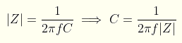
The cap is nominally 22uF. At 8.648MHz, the expected impedance would be given by:
Expected impedance would therefore be 0.84 mΩ. However, the chart indicates that the impedance is 56 mΩ. Based on that, the effective capacitance can be back-worked to be 0.33uF for this 22uF cap!
Now you could say that, this frequency is pretty high and way past the SRF so of course the cap isn't behaving as we expect it to. However, this ties directly to the electrolytic cap I was trying to use too.
When looking at the electrolytic part's datasheet, I noticed no equivalent SRF or impedance information. Electrolytic capacitors are known to have lower SRF than ceramic capacitors, but how bad is it actually?
In summary, consider the construction of a typical electrolytic capacitor where the contact foils are rolled within the package. The images below are taken from the paper linked above.
The current flow through the structure can be modelled as an RC ladder network with distributed resistances and capacitances. This translates to capacitances further down the ladder network (such as C5 shown below) have larger series resistances and the associated time constants are large compared to the period of the voltage across the cap. This results in a drop in capacitance with frequency, greater than that of just the contact and packaging inductances.
A side note of interest is that the opposing current directions through the foils can help cancel the parasitic inductances, asides from small mismatches in foil alignment, depending on device assembly.
Is there an easy way to verify this for the cap I have? And can I trust the 19uF reading from the LCR meter? That's why I proceeded to do. (The reason for the distrust was more due to the meter misbehaving in lab for other measurements but is good to check against.)
Digilent Analog Discovery 2
The following is the required setup to get impedance measurements.
Impedance measurement setup: "Load" is the cap under test
Using this setup, I am now able to get some quick impedance measurements for my cap. A key aspect of this is to perform the short compensation to ensure that measurement parasitics are taken into account. Without performing this compensation at first, I saw very different results due to the ~50nH of additional parasitic inductance through my measurement setup.
The reactance measurement is shown below:
Reactance measurement from 1kHz to 1MHz
I exported the reactance measurements, and then found the values of C0 and L0. C0 is the capacitance at the lowest measurement frequency and L0 is the inductance at the highest measurement frequency. This allows me to simply model the capacitor as a constant C0 in series with constant L0 (and also a constant series resistor but that isn't factored into this reactance measurement).
For these measurements, the values of C0 and L0 are 407.6 uF and 34.5 nH. C0 is within 20% of the 470uF capacitance, as per the part's spec. Overlaying the reactance due to C0 and L0 on the measured reactances yields the following plot.

Parasitic L, C fit on reactance measurements
This shows that barring the area around the SRF, the reactance is very well modelled by the constant C0 and L0. Considering the reactance, then, the equivalent capacitance can be computed as shown below.
"Effective" capacitance fit on reactance measurements
At 100 kHz, the capacitance is about 80 uF and at 200 kHz, the capacitance is about 20 uF! That is a HUGE drop from the 470 uF rating of the part (and measured 408 uF at low frequency). The self resonant frequency is about 40 kHz, which is very low compared to the ceramic cap shown previously. Of course, this is a different part in a different larger package and so that is not a fair comparison.
Back to where I was trying to use this! This is the input cap for a buck converter operating in the 80-200 kHz range. With such a substantial drop in effective capacitance, the input current ripple will be substantially higher than that predicted/computed with a 408uF cap!
In this particular converter, the 408uF cap would lead to about 23 mVpp ripple. However, with a 20uF cap, this goes up to 463 mVpp. Interestingly, operating this converter at a slower 100 kHz with the same cap (80uF @ 100kHz) could result in a lower ripple!
Be careful which parts you use! And make sure you consider the frequency-dependent behavior! Once you're above the SRF, the capacitance value drops precipitously. If possible, operate below the SRF or make sure you understand what the impact will be if you don't. There's also the consideration of ESR but with electrolytic caps, that tends to decrease with resistance - which is why you'll see ripple current specs get better at higher frequencies for electrolytic caps.