
Low-Side MOSFET Drive Circuits and Techniques - 7 Practical Circuits
In many circuits, it is necessary to use MOSFETs for
switching. In many cases, the MOSFET drive signals are generated by
microcontrollers. In other cases, they are generated by ICs – PWM controllers,
timers or any IC in fact. However, MOSFETs cannot always just be connected to
the drive signal and be expected to work properly. Due to the construction of
the MOSFET, driving it is not the simplest of tasks, especially for beginners.
There are many users who regularly ask for help on MOSFET drive related issues
or problems on different blogs, websites and forums. So, here I will show some
MOSFET drive techniques/methods for MOSFETs configured as low-side switches.
Before I head on to MOSFET drive, let me just tell you what a low-side switch is, in case you don't know. When the MOSFET (that you're using as a switch) sinks current, it is a low-side switch. The load will be between the drain and +V supply. The source will be connected to ground. Gate will be driven with respect to ground.
Let me start with N-channel Power MOSFETs. One thing to keep
in mind is that these MOSFETs are fully turned on when the voltage at the gate
with respect to the source (VGS) is > 8V. So while at voltages less than 8V,
the MOSFET will be on (as long as VGS > VGS(threshold) ), the MOSFET won’t
be fully turned on. It will operate in the linear region and there will be very
high losses.
Now let’s go to Logic Level MOSFETs. These MOSFETs tend to
have much lower VGS (threshold) and thus are usually fully turned on with VGS
of 4V to 5V. One downside to Logic Level MOSFETs is that they usually have
higher on-state resistances compared to similarly rated Power MOSFETs. So, this
would mean higher conduction losses for the same load.
Another thing to remember is the gate capacitance. So, when
the MOSFET is to be turned on or off, the gate must be driven high or low with
sufficient current quickly enough so as to charge or discharge the gate
capacitance quickly enough so that the MOSFET spends minimal time in the linear
region and is quickly turned fully on or off. This is true especially for high
speed switching when time period is small. However, in low frequency
applications, this may not be a big problem as, even if the MOSFET spends some
time in the linear region, it will spend the (remaining) majority time fully on
and thus the small amount of time spent in the linear region will not cause
much of a problem.
Let’s first consider the simplest situation: a MOSFET is
driving a load and is periodically turned on and off to turn the load on and
off respectively. How long do I mean by periodically? Well, it really depends
on the application. But for this situation, the period between turning on and
off may be very long or very short but will be at least half a second. A few
examples:
- The MOSFET could be driving a DC fan that will be turned on, kept on for 2 hours and then kept off for about an hour and turned on and off in few hour intervals.
- The MOSFET is driving a DC lamp that will stay on for the entire night and will only be turned off in the morning and kept off during the entire day.
- The MOSFET is driving a heating element through which current passes (the heater is on) for about 16 hours a day.
- The MOSFET is driving an IR LED in a remote transmitter unit. The LED is turned on and off frequently – every few seconds.
So, the above examples should clarify what I meant as
“periodically” in the preceding paragraph.
In such situations, MOSFET drive is simplest – apply a high
enough voltage to the MOSFET gate and the MOSFET will be on; ground the MOSFET
gate and the MOSFET will be off. Quick charging and discharging of the MOSFET
gate capacitance are always desirable. But in this situation, the charging and
discharging need not be very quick as frequency isn’t high.
Here are a few circuits that can easily be used.

Fig. 1 (Click on image to enlarge it)

Fig. 2 (Click on image to enlarge it)
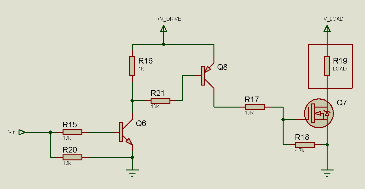
Fig. 3 (Click on image to enlarge it)
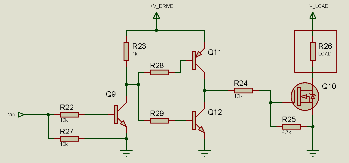
Fig. 4 (Click on image to enlarge it)
In each of these circuits Vin is the input drive signal to
the MOSFET. +V_DRIVE is the voltage supply to drive the MOSFET. When the MOSFET
is on, VGS = +V_DRIVE. When the MOSFET is off, VGS = 0. MOSFETs have a maximum
rated VGS. For most MOSFETs, this is 20V. For some it is higher up to 30V.
There are MOSFETs (usually Logic Level) which have a lower maximum rated VGS. It
is always best to check the datasheet for the specific MOSFET being used.
Fig. 1 shows an inverting driver. Here, the MOSFET is turned
on when Vin is low and turned off when Vin is high. When the MOSFET is on, the
load is on and vice versa.
Fig. 2, Fig. 3 and Fig. 4 show non-inverting drivers where
the MOSFET is turned on when Vin is high and the MOSFET is turned off when Vin
is low.
In Fig. 2, the MOSFET turns off almost instantaneously when
Vin is zero. This is because when Vin is zero, Q3 is off and Q5 is on. Q5 pulls
the gate low, discharging the gate capacitance. However, the MOSFET turn-on is
not instantaneous. When Vin is high, Q3 is on and Q5 is off. So, current flows
through R14 and charges the MOSFET gate. Here turn-on time is dictated by R14.
However, when I say long turn-on time, I am talking in the order of tens or
hundreds of microseconds to milliseconds at max. Thus this circuit can easily
be used in any of the situations depicted in the four examples above or any
similar situation. This driver cannot
be used when switching is done in the order of microseconds where both turn-on
and turn-off must be very quick – almost instantaneous.
In Fig. 3, the MOSFET turns on almost instantaneously when
Vin is one. When Vin is one, Q6 is on and so Q8 is on and thus VGS = +VDRIVE
and so the MOSFET turns on. However, when Vin is zero (and so Q6 and Q8 are
off), the MOSFET gate discharges through R18. So, gate discharge is slow and turn-off
time is dictated by R18. However, this “slow” time is in the same order as
mentioned above and so can be used in any of the situations depicted in the
four examples above or any similar situation. Similarly, this driver cannot be used when switching is done
in the order of microseconds where both turn-on and turn-off must be very quick
– almost instantaneous.
In Fig. 4, both turn-on and turn-off are very quick. This
driver can be used for higher frequencies than can the other three.
If the MOSFET is a Power MOSFET, +V_DRIVE should be at least
8V. A voltage commonly used is 12V. +V_DRIVE should be less than VGS(max) as
specified in the MOSFET datasheet. Some “headroom” should be used. So, if
VGS(max) is specified as 20V in the MOSFET datasheet, it is good practice to
use lower than 18V. 12V and 15V are commonly used for Power MOSFET gate drive.
For Logic Level MOSFETs, 5V is most common because the reason a Logic Level
MOSFET is usually used instead of a Power MOSFET is that the Logic Level MOSFET
can be driven from 5V. In the above shown circuits, the MOSFET can be either a
Logic Level MOSFET or a Power MOSFET. +V_DRIVE must be selected accordingly.
Each of the above four circuits requires only a minimum
voltage of 0.7V to fully turn on the MOSFET (+V_DRIVE must be selected
properly). Each of the above circuits can also be used to drive either Logic
Level MOSFETs or Power MOSFETs.
Here are a few more circuits that I’ll discuss below.

Fig. 5 (Click on image to enlarge it)
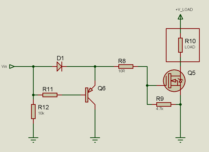
Fig. 6 (Click on image to enlarge it)
Fig. 5 and Fig. 6 both show non-inverting drivers.
The driver in Fig. 5 has the advantage that, while being simple,
it can both quickly turn on and turn off the MOSFET. In the drivers in Fig. 1, Fig.
2, Fig.3 and Fig. 4, when the MOSFET is on, VGS = +V_DRIVE. The MOSFET is turned
no when Vin is at least 0.7V. So, that means that when Vin is higher than 0.7V,
VGS = +V_DRIVE. So, for example, if +V_DRIVE is 12V, VGS will be +12V, when Vin
= 3.3V, 5V, 9V and so on.
However, in the drivers shown in Fig. 5 and Fig. 6, when the
MOSFET is on, VGS = Vin – 0.7V. So, that means that in Fig. 5, even if +V_DRIVE
is +12V, when the MOSFET is on, VGS will only be equal to Vin – 0.7V and not +V_DRIVE.
So, for Fig. 5 and Fig. 6, if +V_DRIVE is +12V and Vin = +5V, VGS will equal +4.3V
when the MOSFET is on.
That is the disadvantage to these circuits – that the MOSFET
VGS will depend on the magnitude of Vin. However, there are situations where these
disadvantages do not matter.
If the MOSFET is a Logic Level MOSFET that is to be driven by
a microcontroller, then the driver in Fig. 5 can be used quite easily. When Vin
= +5V (typical output of a microcontroller), the MOSFET will be turned on and VGS
= +4.3V. Remember that +4.3V is enough to fully turn on the MOSFET. When Vin = 0,
VGS = 0 and the MOSFET will be off.
You may, then, ask why a driver is needed. You may simply drive
the microcontroller directly from the microcontroller. And well, you can. For low
speed applications. So, in the four situations previously described, the microcontroller
can directly drive the Logic Level MOSFET. The problem lies where the microcontroller
output voltage will drop when supplying the current needed to quickly turn the MOSFET
on and off when a large current will be required. So, the MOSFET may not fully turn
on. In that case, the driver shown in Fig. 5 can be used to ensure that the MOSFET
can be driven with sufficient current.
The driver in Fig. 6 can be used when the control chip can only
source current but cannot sink current. One example is the SG3524 PWM controller
configured to source current. The 0.7V drop is not a problem since the outputs of
the SG3524, when high, go up to near the supply voltage. So, even after the 0.7V
drop, the voltage is sufficient to fully turn the MOSFET on.
The driver in Fig. 5 is commonly used to drive a MOSFET from
a PWM controller. Usually the outputs of PWM controllers go all the way up to the
supply voltage (usually 12V, 15V, etc). So, this driver can easily be used, because
even after the 0.7V drop, the voltage is high enough to fully turn on a MOSFET.
The transistors can also supply high currents. This type of driver based on such
a combination of transistors is called a totem-pole driver.
Till now, I’ve only talked about low frequency applications.
Now let’s move on to high frequency applications.
One thing that must be considered in high frequency applications
is the MOSFET drive current. When frequency is high, time period is low. So, the
MOSFET must be turned on and off in a short time to avoid high losses. The turn-on
and turn-off times must be as short as possible to ensure that the MOSFET will be
in the linear region for minimum time.
Thus it is natural that to minimize gate charge time, current
must be maximized. So, the quicker the gate must be charged or discharged, the higher
the charge or discharge current should be. The drivers in Fig. 4, Fig. 5 and Fig. 6 can be used for high-frequency MOSFET drive.
I’ve covered some discrete drivers here based on transistors.
However, I always recommend using dedicated driver chips for driving Power MOSFETs
in high-frequency applications. Low-side drivers are easily available at low prices.
One widely available low-cost low-side driver (that I often use) is the TC427.
The circuit using a TC427 is very easy. The supply voltage has
to be provided to the supply pins. Then, all you need to do is provide the input
signal and just drive the MOSFET from the TC427 output. The TC427 has 2 drivers.
So you can use the TC427 to drive 2 MOSFETs from 2 different input signals. Here
is the circuit diagram:

Fig. 7
As you can see, the circuit is very simple. +V is the supply
voltage. MOSFET drive voltage swings up to about VDD - 0.025V when MOSFET is to
be driven high and down to +0.025V (can be assumed to be zero as this is way below
MOSFET VGS(threshold) when MOSFET is to be driven low.
Download the TC427 datasheet from here:
There are numerous ways to drive a MOSFET in a non-isolated low-side
configuration. I’ve shown a few circuits using transistors and one using a dedicated
driver.
You can find loads of driver chips and the datasheets should
show the circuit diagrams. Here I have only covered low-side non-isolated drive.
I shall soon make another tutorial where I cover high-side drive and isolated drive.
I hope that this tutorial has helped you. Let me know your comments
and feedback.


What are the values if resistances used in figure 4?
ReplyDeleteYou can try with a range of values for R28 and R29. 1k is okay. For low frequencies, even 10k may be okay.
ReplyDeleteIf R28,R29 are too low (i.e. values comparable to R23) then the resistors will cause loading of the previous stage. This will cause the voltage at bottom point of R23 to hover somewhere between 0 and V+ rail. If this happens the output npn-pnp pair will conduct simultaneously (in linear mode) and cause heating up and possible burn-out of the pair.
DeleteOn the other hand using excessively high values will cause a problem with the switching of the MOS gate, because the maximum available output current from the npn-pnp pair will be lesser (lesser maximum base current available etc.). With R28,R29 values of 10K and R22 of 4K7 with off-the-shelf npn and pnp transistors (BC547,BC557) the rise/fall times at the output MOS gate is around 250nS for 3A load and 6V supply, for a IRFZ44N MOSFET.
This means that it should be useable to upto around 1kHz (rise/fall time << 1/10th of waveform period), Practically this is safe to use upto around 2kHz or so at around 4A and 6V drive voltage available, provided you've a reasonable heatsink on the MOS (For IRFZ44N).
You agree Tahmid?
Yes, you have to ensure that R28 and R29 are high enough that you don't cause loading of the previous stage. You'll have to ensure that you can keep the transistor in saturation mode, so that the collector voltage of Q9 is always V_DRIVE or zero but not in between or you risk turning both transistors on.
DeleteYou can also improve this by increasing transistor drive current.
I'll run some simulation tests to get some numbers.
Hi , what value should I use for R28 and R29 if V_drive is around 14V and load current around 25-30A(it's a motor).
Deleteone disadvantage is there in fig:4 .
ReplyDeleteif Vbe of Q11=8v and vbe of Q12=8v .so at that time both transister become on , may occure damage .
but vbe of both transistor should not come 8v ,and which have only 0v or 12v ,anyway if it happend then transister bcme damage .Right?
Yes, what you have said is correct. If +V_DRIVE is +12V and voltage at collector of Q9 is 8V, then there will be cross-conduction : Q11 and Q12 will both be on and there'll be a short-circuit. However, there is no scope for the collector of Q9 to be at 8V unless R23 is very small, which it shouldn't be. With 1k as shown, there'll be no problem.
ReplyDeleteif Vin is <0.7v then collector of Q9=12v , if >0.7v then it is 0v . ok am agree .
ReplyDeleteBut if Vin is =0.7v what will happen . and we can't say it may one of the state in 0 or 12 .
i think it will be in between 0 and 12 [so both transitor become on Q11 and Q12]. because transister haven't any sharp cut of voltage for vbe=0.7v, and this value will vary for each transtr.
So for a deep thinking Pure designer will not accept this circiut[fig ;4]. right tahmid?
For simplicity's sake it has been considered that VBE = 0.7V but you must keep in mind that this is a property of the transistor and may vary depending on the transistor, although it should usually be around 0.7V (or 0.6V).
ReplyDeleteAt certain voltages, it may cause problem. But, the input shouldn't ever be 0.7V since it will come from an IC or microcontroller, whose output when high is never 0.7V but nearer the supply voltage, due to which this problem is never faced practically.
And that is why, this circuit is accepted and also used in many commercial circuits, even in India.
agree thamid thanks .
ReplyDeletecan you give me your email id?
my id : ismailpp2008@gmail.com
Hi,
ReplyDeleteMy email ID is inferno-rage (at) hotmail.com
hi thamid
ReplyDeletein above u r mentioned about low side driver and its relatives, But Can you explain how its related to High side driver circuit?. with simple example . And pls explain Which mos is good for low side and which one is for high side Ie: n- channel /p-channel.
I will soon write up an article about high side drive. Currently I am quite busy. Once I'm free, I'll write some more articles/tutorials.
ReplyDeleteI've written an aricle on high-side and low-side drive using IR2110. Perhaps doubts regarding high-side drive, at least those regarding IR2110, will be cleared if you check it out:
ReplyDeleteUsing the high-low side driver IR2110 - explanation and plenty of example circuits:
http://tahmidmc.blogspot.com/2013/01/using-high-low-side-driver-ir2110-with.html
Regards,
Tahmid.
Hi Tahmid, Its Mehdi from dhaka, I made a circuit for solar charge controller using N-Mosfet and some drive components. It works for 12 volt system but problem when drive for 24 volt system. If I could sent it for you, then may be you can help me. Do I have your email ID or phone no? My email : mehdi98_here@yahoo.com, cell: 01713112249
ReplyDeleteBest Regards
Mehdi
Hi,
DeleteMy email address is inferno-rage (at) hotmail.com
However, I recommend you upload the schematic to a file storage server such as rapidshare. Everyone can benefit if the discussion goes on here.
Regards,
Tahmid.
Hi mehdi and thahmid ,
ReplyDeletei have same problem when i am using 24v for charger , i have just convert 24v to 12v using 7812 ,
But 7812 getting damage instantaneously.
please go through this link, i have updated that issue in edaboard :
http://www.edaboard.com/thread281331.html#post1204711
In situations where there is a large voltage gap between input and output, I always recommend using switching regulators. Some common regulators include the LM2575, L4971 (this one's cool because it's in an 8-pin PDIP package), L4962, etc.
Delete___________________________________________________________________________________
I've replied to the edaboard thread as well.
___________________________________________________________________________________
Regards,
Tahmid.
Thanks Tahmid for your reply. I got my problem. It was nothing but the ground reference. I tied both battery positive and solar positive together and tried to switch on ground lines. Battery connected to the mosfet drain and solar connected to the source. As driving for 12V system both voltage level are same but when driving for 24 volts there's the problem because I supplied the drive power from 12V battery with ground from battery. Now I drive mosfet gate with reference to solar ground and no problem. I will upload the circuit very soon.
ReplyDeleteThanks you guys again.
Mehdi
Glad to hear that you've fixed it!
DeleteRegards,
Tahmid.
Hi Tahmid,
ReplyDeleteThe MOSFET IRFZ44V heated much when I used this in Buck converter (during low pulse only). Its gate volt is 4.64. What might be the problem?
Thanks.
Mitz
Is 4.64V the average voltage or "peak voltage level"? You should upload the schematic, especially of the driver. Upload it to an online file storage site, such as rapidshare. Make sure you make the file "public".
DeleteRegards,
Tahmid.
What is the purpose of having 10k resistors to pull down mosfet driver input ? Are they required ? Also may I ask what kind of resistors and values you are using between mosfet driver and mosfet gate ? I see on schematic you posted 10 ohm resistor, but how you found that particular value ?
ReplyDeleteSorry, one more question if you don't mind : what kind of capacitors can be used for decoupling mosfet driver ? Some datasheet propose film capacitors but MKP types are rated for much higher voltages and are big, can I use tantalum capacitor here ? (I'm trying to use smd components)
The 10k pull down resistors have been used to ensure that no input pin is floating, so thatstray noise is not picked up.
DeleteFor the gate resistance, usually values between 4.7 ohm and 22 ohm can be used. 10 ohms is a common value that can work. For high frequencies (100kHz and above), you may need to reduce that to about 6.8 ohms. For more detail regarding the gate resistance, refer to this:
http://www.edaboard.com/thread221750.html#post943534
For low capacitance (eg 100nF) decoupling capacitors, ceramic types are the best. Try to use ceramic disc capacitors instead of tantalum capacitors. You should be able to easily get 50V ceramic disc capacitors. Like these:
http://uk.mouser.com/Passive-Components/Capacitors/Ceramic-Capacitors/Ceramic-Disc-Capacitors/_/N-5g90?P=1z0x83k&Keyword=100nf&FS=True
Hope this helps.
Regards,
Tahmid.
jajha kumullah khair,
ReplyDeleteit has broaden the door to entering in the power electronics world for the beginners as me
Hello Tahmid I have been following your tutorial all along even in other forums. i am trying to build a 1000 watt inverter to run my fridge but having great problems. I built fig 5 as my driver for irfz44 fets in my dc to dc converter but as u say u need about 8v to fully turn on the fets. I want to know if I should have this voltage on the gate of the fets when there is no load on the output of the h bridge. Please clearlt tell me if this voltage should be there at all times. This is my question I have been trying to get an answer for for the past two months. Thank you
ReplyDeleteRemember that the circuits shown here are for low-side MOSFET drive and so should not be used for H-bridge drive unless you're using them for driving the low-side MOSFETs in the H-bridge.
DeleteTo drive the MOSFET fully on (with or without load), the gate of the MOFSET should be at least about 8V higher than the source. However, if you don't have a load, the circuit is incomplete and it doesn't matter if the MOSFET is on or off. But, considering that a load may be applied at any time, since it's an inverter, the voltage on the gate must be present whenever the MOSFET is to be on.
I hope that answers your question.
Regards,
Tahmid.
DEAR Tahmid
ReplyDeletei need your help
i have 4 n-channel igbt (G40N60) , i connected them in H-Bridge
can i drive them using driver circuit shown in fig.4 ??
i use pic16f377A to generate squre wave
The circuits I've presented here are only for low-side MOSFET/IGBT drive. You can use the driver circuit shown in Fig. 4 only to drive the two low-side IGBTs. However, I recommend you use dedicated high-low side MOSFET/IGBT drivers such as IR2110 to drive all the MOSFETs.
DeleteRefer to this tutorial that I've written:
Using the high-low side driver IR2110 - explanation and plenty of example circuits
http://tahmidmc.blogspot.com/2013/01/using-high-low-side-driver-ir2110-with.html
Regards,
Tahmid.
hello Tahmid keep the good work gooing. I have a question can i use fig 4 to drive a pushpull stage for a transformer base output inverter running at 50hz. Thank u for ur support
ReplyDeleteYes, you can. The push-pull stage consists of 2 MOSFETs (or 2 sets of paralleled MOSFETs) that are both low-side. So, you can use that circuit.
DeleteRegards,
Tahmid.
thank u very mucg Tahmid because I tried fig 1 but only got about 6.80v at the output and when I connect it to my pushpull config it just caused the transformer to make a heavy sound and cut the ac volts
ReplyDeleteWhat's the frequency of the driving signal and the duty cycle? What's the supply voltage?
DeleteWhere does the driving signal come from?
thank you for your reply the drive frequency is 60hz coming from a sg3524 and i was using 12v to supply the drive circuit in fig 1
DeleteCan you check the output waveform with an oscilloscope and post the pictures?
DeleteIf you're using the SG3524 powered off 12V to generate the signals, the voltage you measure shouldn't be more than 6V, as maximum duty cycle should be 50%.
12V * 0.5 = 6V
Are you using your voltmeter to measure the voltage at the SG3524 outputs?
hello Thamid one more question if I use the tc427 to drive my pushpull output inverter and use a supply volt of 12v for the tc427 would my vgs volt to thefets be also 12v thank u
ReplyDeleteVGS when the MOSFET is driven on would be about 0.025V below 12V (VDD - 0.025V).
DeleteAverage voltage registered by the voltmeter would be (VDD - 0.025V) * (Duty Cycle).
Regards,
Tahmid.
thank you tahmid . I am building this transformer output inverter but the sg3524 is only puting about 3.3v on the gates and as from other blogs u said the fets should be getting about 8 or 10v to fully turn on I am using irf260n so I think I need a drive circuit. Is this correct. Thank you fro ur support
DeleteIf you're using a voltmeter to measure the output from the SG3524, you're only reading an average voltage. The voltage that matters is the amplitude.
DeleteThat being said, the SG3524 doesn't have a totem-pole driver, but only either a current source/sink. So, you should use a MOSFET driver anyways when using the SG3524.
Regards,
Tahmid.
Hi, am designing using proteus 7.7 on a 0.5hp, 415v induction motor drive. I'm making use of 6 1200v IGBT switches but i'm currently having a problem with the drivers available in proteus. I therefore want to know if it's possible to use 600v drivers for these switches.
ReplyDeleteIf your maximum supply voltage is less than about 500V, you should be able to use the 600V drivers. It's the maximum supply voltage that matters when selecting the driver and not the voltage ratings of the IGBTs. You could very well have used 900V IGBTs or even 2000V IGBTs, but the supply voltage would still be the same.
DeleteRegards,
Tahmid.
Hello Tahmid.
ReplyDeleteI am using the TC427 to drive the low side N-mosfet from H-bridge.
The P-mosfet from high side is on. (I am only testing one direction of the bridge)
When I start, stop the motor the TC427 burned. Now I am using the 4 diodes in the H-bridge
and the new TC I use is alive.
It is so easy to burn them?
The P-mos is IRF4905, the N-mos is IRF3205.
I will design a high bridge and I am afraid that the TC will get burned easy.
What may be the cause?
If you could let me some mail I can send you the circuit.
Thanks!
Sebastian.
Hello,
ReplyDeleteI'm curious in R23 in Fig4. If I manage to get the resistance so high (let's say it's much higher than CE junction of Q9 when it's cut off if I can get a hand on), will the collector of Q9 always give only 0V without Vin=5V input?
There needs to be a minimum collector current flowing to ensure proper operation of the transistor and to get 0V at collector when Vin = 5V. The collector current must be greater than ICEO (specified in the datasheet). So this means that you can't pick a resistance (for R23) too close to the resistor of the CE junction, let alone higher. In fact it should be at least 10 times less in order to ensure proper operation. Of course this 10 times isn't a hard set rule, but something you can do to avoid problems.
DeleteYou need to factor into the collector current due to pulling in the PNP base as well.
DeleteAlso do remember you need to be able to supply enough current from this stage so that the PNP transistor in the next stage can supply high currents to drive the MOSFET if required.
If there is no R25 in Figure4 and the gate voltage of FET become zero, will the discharged charges from Gate-Source internal capacitance damage the FET?
ReplyDelete(cuz zero gate voltage is equal to source voltage which is grounded. Without R25, can we imply that the gate is shorted with the source? or it's just a virtual short circuit and there is no discharged current?)
If there is no R25, there should (ideally) be no problem since zero gate voltage, like you said, means that the gate is at source potential and the gate is "shorted" to the source. Even with R25, this is what happens with the transistor pulling the gate low. The importance of R25 is not to turn the MOSFET off but rather to prevent it from accidentally turning on due to the drain-gate parasitic capacitance. Read here: http://tahmidmc.blogspot.com/2012/10/magic-of-knowledge.html
DeleteHow i can replace a relay driven by a PIC with a Mosfet.
ReplyDeleteThe load is 24VAC / 2Amps ?
Google 'solid state relay with MOSFET'.
DeleteHello, can i use na dc motor after de mosfet?, Ex, in a car, the dc motor is grounded, so de mosfet needs a P Chanel, but i can use a N Chanel with the dc motor after, and a driver transistor ? example circuit? (sorry, i don,t speak english...) Thanks, estevamfreitas@bol.com.br
ReplyDeleteYou can put the load between drain and supply voltage and operate the N-channel MOSFET in the low-side to drive the load. If you want to use the N-channel on the high-side, you'll need to use a high-side driver. The choice of driver will be dictated by your required duty cycle, etc.
DeleteI am thinking of using circuit 7.I have a problem.I never understand the ground connections.The output of microcontroller is fed to TC427 as input.Should the ground of micro controller be shorted with the ground of the chip,TC427.
ReplyDeleteTC427 is a non-isolated driver. So it must share the same ground connection as the microcontroller.
DeleteHi i checked the circuit in fig.4 but in order to switch the mosfet fast " 60nS "like irlr2905 we need a high current going through the bjt. with R23 1K and supply of 12V we have 0.012A going to the bjt pair. does the 0.012A open the irlr2905 fast ???
ReplyDeleteWe simulated with r23 160Ohm for 0.075A collector current and R28 R29 500Ohms and on sim it get 50nS to for the Voltage across irlr2905 to go from 24 to 0V, but it takes 500ns for the Vgs to go from 200mV to 12V or 300ns to go from 200mV to 10V.
Are the values i selected for R23, R28 and R29 correct???
Do you want the turn on and turn off times as close to 60ns as possible? Which BJT are you using? Is it a standard BJT or a darlington pair? After knowing the gain (hfe) of the BJT, some simple calculations will give the required values.
DeleteHi Tahmid
ReplyDeleteCould you please let me know if an optocoupler is required between the Microcontroller (Arduino Due) and IR2110 Mosfet Driver. Thanks in advance.
Hello Tahmid thank u for ur help here . I have a question could I configure fig4 with a boost cap and use it as a high side driver will it work as how it works for low side . I await ur reply
ReplyDeleteCan I use Fig4 driver for driving high side N channel mosfet with V_drive = ~20v and V_load = 12v ?
ReplyDeletethanks
Hi Tahmid
ReplyDeleteIn fig 5,You say VGS =Vin-0.7v,then if +V-Drive=12v and Vin=5v.Surely 5-0.7(Base,emmittter of Q1)=4.3v turns Q1 on?Then 12v goes through to Gate of Q2 and turns the Fet on?
I can't figure out why in the top four figures if Vin>0.7v it switches +vDrive through to the gate of the fets but in fig5 it does'nt
Regards Robin
hi tahmid
ReplyDeletei am working on two switch buck-bost converter. i am using irfp460 power mosfet.This converter requires the use of two active switches and is designed by combining a buck converter and
boost converter design in the same topology. Due to this design this converter can work as Buck-only,
Boost-only or Buck-Boost converter. The input voltage source is connected in parallel with diode D1,
MOSFET Sboost, load capacitor, C. MOSFET Sbuck is connected between the input
voltage source and diode D1. The inductor is connected between D1 and Sboost, while D2 is connected
between Sboost and the output or load capacitor.
please tell me which side of gate driver i use for sboost and sbuck. also tell me about optocoupler hcpl-3120.
Hi Tahmid,
ReplyDeleteNice to see this blog. I am facing a problem using ICL7667. This ic is similar in pin configuration like fig 7. With the input B grounded and nothing connected at the output the IC is heating up too much. I have burned one IC. What could be the possible cause.
Hi tahmid,
ReplyDeletei need your support. what is the value of resistor R9 (10R) in the Fig 2. i placed 10K resistor for R9. I have connected a load (Pneumatic actuator) which operates in 12V (211mA max). but the actuator is not opening. the voltage measured at gate of MOSFET is 11.5V fro the collector of 2nd emitter follower transistor in circuit diagram.
Thanks Tahmid,
ReplyDeleteYour blog is very informative & helpful.
Can we get same performance using discrete components driver as that of special driver ICs? These ICs are costly.
how we can determine the resistance from frequency and capacitor
ReplyDeletehow we can determine the resistance from frequency and capacitor
ReplyDeleteHello Tahmid,could you please let me know How I can increase the low voltage from the PIC to 15V so that I can control my IGBT (IRG4PC50FD),it is writen in the datasheet that it requires 15V as VGE and I want to control the full bride three phase system driven with SPWM from PIC16F1936,I have the IR2110 and TC427 Drivers only could you please advise on how I can proceed for controlling my AC three phase induction machine?
ReplyDeletePlease help.Thank you!!
very well written, thank you!
ReplyDeletehi bro. Can you plz refer me a high frequency switching mosfet which able to detect approximately 20Mhz output...
ReplyDeletehi tahmid, could you explain me how the totem pole works in fig 5
ReplyDeleteHi Tahmid, very illustrative examples, in the fig. 4; how can I do if I have a bipolar power source (+) & (-) in the hv side? should I connect the (-) to common earth in order to have a same circuit reference?
ReplyDeletehello.... can u please tell me how to drive 6 MOSFETs (IRF 3205 or MTP 75N06)? 3 MOSFETS ON PIN NO.14 AND OTHER THREE ON PIN NO. 11 OF IC SG3525A.
ReplyDeleteAssalam Alakum
ReplyDeleteDear تحميد
how to build a H-Bridge by using the Figure5 in this blog page)
Thanks
(http://tahmidmc.blogspot.com/2012/12/low-side-mosfet-drive-circuits-and_23.html
Thank you for this, its been very helpful for me.
ReplyDeleteHello,
ReplyDeleteThanks for taking the time to explain this topic so clearly! Much appreciated. Can you tell me, in what situations do you use a P-Channel Mosfet? Is it a personal preference of yours not to use P-Channels?
Thanks,
Sean
Well said and it is really true...
ReplyDeleteNews stories and feature articles are more authentic
and credible than advertisements to readers.
The articles act as testimonials. The message
gets through to the potential buyers as news and
they may not turn away from it as they turn away from the advertisements.
You deserve appreciations. I really learned a lot from it. Keep it up.
top web designer company in india
top seo service company in india
Hello Tahmid,
ReplyDeleteIs it possible to drive ir2110 from a function generator => Lin positive lead, VSS negative lead ? I’m not sure I understand how to wired ir2110 with function generator.
That brings the other question => Why using ir2110 if you have a function generator?
Best regards
Hi,
ReplyDeleteThanks for sharing a very interesting article about Low-Side MOSFET Drive Circuits and Techniques - 7 Practical Circuits. This is very useful information for online blog review readers. Keep it up such a nice posting like this.
From,
Retailmass,
POS Billing Software
This comment has been removed by the author.
ReplyDeleteHi,
ReplyDeleteThanks for sharing a very interesting article about Low-Side MOSFET Drive Circuits and Techniques - 7 Practical Circuits. This is very useful information for online blog review readers. Keep it up such a nice posting like this.
From,
Maestro Infotech,
Best Web Design Company in Bangalore
I am using sg3525 ic for driver and mosfet irf3205, ferrite transformer for push pull topology but both mosfet blown after 3 sec please suggest. winding details are primary side 0.6X5mm 3+3 turns, secondry 0.6mm 90 truns.
ReplyDeletecore size ETD 50
This comment has been removed by the author.
ReplyDeletethank you very much for your interesting article.
ReplyDeletequesion1 about the gate current: why the driver of Mosfet must delivrate more current, i think that Mosfet-gat need only voltage and very low current consumtion to be on/off.
Q2-Mosfet Can burned by using Gate-Voltage lower than full-openning voltage(8v) in situation of high Current load.
Q3-what is the best choice of Mosfet and it driver when we have ignition-coil load with 450 voltage /current unknown
Thanks Tahmid, very nice topic... keep it up!
ReplyDeleteHi!!! I need to construct the high frequency (approximately 40Mhz) half bridge circuit for my fer-rite core transformer. What is the suitable MOSFET driver and the type of MOSFET??? Please me suggest the suitable circuit design for it....
ReplyDeleteI would like to know if this application not is also applicable with IRS2186?
ReplyDeleteCan i use this circuit for invertor(dc to ac)?
ReplyDeleteCan i use this triggering circuit for trigger MOSFET(IRF3205)?
ReplyDeleteI suggest swapping C1 and C2 in Fig. 7. Put the small ceramic cap closer to the IC. minor nitpicking ;).
ReplyDelete